

AmTECH bridges R&D innovation with scalable, sub-micron packaging for photonics, medical, neuromorphic, quantum and DoD applications.
AmTECH Team: David Walter Chavez
In today’s Industry 4.0 landscape, innovation is advancing at unprecedented speed, but many promising
ideas still fail to scale beyond early prototypes. This critical gap, known as the “valley of death,” occurs
when startups face the dual challenge of securing funding while needing access to advanced manufacturing
capabilities. Too often, companies stall at this inflection point, lacking the infrastructure to move from
proof-of-concept to commercial production. AmTECH Microelectronics exists to bridge that divide by
providing on-shore, state-of-the-art facilities equipped with sub-micron flip-chip placement, automated
wire bonding, and soon, active alignment for next-generation products. The company’s model supports
startups and innovators in transitioning from lab-fab by building pilot production lines, ensuring that great
ideas are not lost to manufacturing bottlenecks. By partnering with AmTECH, companies gain both the
technical expertise and scalable infrastructure needed to cross this chasm. AmTECH bridges the valley of
death by transforming early-stage prototypes into commercially viable products through advanced on-shore
packaging capabilities.
The government’s initiative, the Microelectronics Commons, and its various chapters aim to bridge this critical gap by bringing academia and government projects funded by the DoD into closer alignment with industry partners. Nevertheless, challenges remain, and the supply chain will take time to fully mature. As the Department of Defense has noted, “Today, microelectronics designs that are proven within U.S. universities and businesses of all sizes frequently do not enter large-scale production because the transition from laboratory to fabrication is notoriously difficult; a high technology readiness does not mean high manufacturability. The Commons is focused on easing this transition for microelectronics that are essential for our national security.”1 AmTECH is proud to be a member of the Pacific Northwest AI Hub, a sub-organization of the Microelectronics Commons led by Dr. H.-S. Philip Wong and Dr. Tsu-Jae King Liu. At the most recent member committee meeting held at Stanford University, AmTECH was encouraged to engage with many academic leaders developing technology roadmaps and preparing proposals for DoD and CHIPS & Science Act funding to advance new CMOS+X products.
The Road to Commercialization
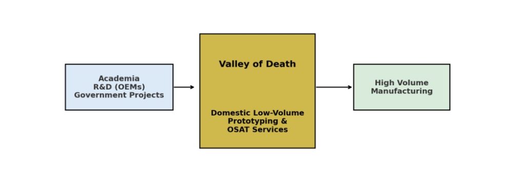
Figure 1. Conceptual diagram of the “Valley of Death” in semiconductor commercialization,
highlighting the role of domestic prototyping and OSAT services.
Most high-volume subcontractors avoid the ‘valley of death’ stage, leaving companies to ask: where can I find an on-shore OSAT that embraces collaboration and co-development, offers state-of-the-art equipment, and delivers prototype through low-to-medium volume production with fast, cost-effective turnaround? In his early 2025 article First-Time Silicon Success Plummets, journalist Ed Sperling observes that “first-time silicon success is falling sharply due to rising complexity, the need for more iterations as chipmakers shift from monolithic chips to multi-die assemblies, and an increasing amount of customization that makes design and verification more time-consuming.”2 Today’s chip designs are larger, more heterogeneous, and increasingly reliant on chiplets, 3D-ICs, and complex software stacks. These factors have driven verification demands beyond what schedules can accommodate, with roughly 70% of re-spins traced to specification errors and many companies anticipating multiple iterations. This cycle of complexity and respins places enormous pressure on design teams, especially during the high-iteration, low-to-medium volume development phase. As a U.S.-based semiconductor packaging supplier with decades of expertise, AmTECH helps ease this burden by providing rapid, reliable packaging solutions tailored for frequent design revisions. Sperling’s so-called “Productivity Gap 2.0” is unlikely to disappear anytime soon, and the industry must adapt in order to survive.
Intellectual property and security concerns have long been a polemical topic in discussions of novel technological developments. Although offshore production may offer more agreeable prices, the long-term negative externalities of property theft and the risks involved are not beneficent to the United States semiconductor ecosystem. A 2023 journal article co-written by personnel at the University of Miami and Florida State University cites the following statistic: “Despite the significant push in bringing chip fabrication onshore, it’s also essential to devote the same amount of attention to building onshore capabilities of advanced packaging in the US to fully secure the semiconductor supply chain. This technical analysis identifies advanced packaging, particularly heterogeneous integration (HI), as a crucial enabler of continued semiconductor innovation amid Moore’s Law slowdown. However, the US currently accounts for only 3% of the total advanced packaging market share, and the rest of the packaging is done offshore, which may cripple the semiconductor supply chain.”3 This point further substantiates that many innovators in the United States face a rift in seeking advanced technology processes onshore, with barriers to entry including limited high-skilled labor and insufficient access to cutting-edge equipment, ultimately leading to bottlenecks in the supply chain.
2 Ed Sperling, “First-Time Silicon Success Plummets,” Semiconductor Engineering, March 27, 2025.
What sets AmTECH Microelectronics apart from other industry players? Its unwavering commitment to collaboration. Rather than pursuing exclusivity, the company has co-developed processes alongside partners and customers, creating a model that accelerates innovation and builds trust. AmTECH continually reinvests in state-of-the-art equipment, skilled personnel, and modern facilities to stay competitive and serve the most advanced technologies. A research paper written by colleagues, Mohamed Cherif and Walter A Chavez, exemplifies the company’s expertise on higher density packaging technologies in SIP, MCM, and chiplets; “Sub-micron flip chip alignment (0.5–0.3 µm) is critical for customers operating at the forefront of technology, where even the slightest misalignment can compromise performance. Quantum computing companies require this level of precision to ensure accurate optical coupling and low-loss signal transmission in photonic and superconducting circuits. Lastly, R&D labs and advanced semiconductor startups engaged in 2.5D/3D integration or neuromorphic systems require sub-micron placement to support ultra-fine pitch interconnects and emerging device architectures.”4 AmTECH’s participation in industry forums like IMAPS, GOMACTECH, and ECTC has reinforced its awareness of the growing demand for advanced packaging requirements, heterogeneous integration, and co-packaged optics for energy efficiency. These insights guide the company’s strategic investments and ensure that it remains aligned with the trajectory of cutting-edge semiconductor technologies. As AmTECH looks forward, it maintains that true competitive advantage by forging relationships and working as a team.
The semiconductor industry continues to grapple with a persistent gap between invention and innovation, particularly in the transition of research-driven concepts into manufacturable products. Early-stage companies and R&D teams across the United States still struggle to secure advanced manufacturing partners capable of supporting prototype and low-to-medium volume production. While the government seeks to establish organizations to train high-skilled labor and distribute funding across institutions that can support high-volume manufacturing, many promising ideas are nevertheless lost in the ‘valley of death.’ The so-called ‘valley of death’ represents the perilous translational juncture at which early designs and prototypes must be systematically engineered, iteratively refined, and rendered manufacturable at scale as defined by both technical and financial stakeholders. By standing at this critical intersection, AmTECH ensures that groundbreaking ideas do not wither in the valley of death but instead advance into manufacturable technologies that bolster both industry progress and U.S. competitiveness.
3 Rouhan Noor et al., “US Microelectronics Packaging Ecosystem: Challenges and Opportunities,” arXiv, arXiv:2310.11651, October 30, 2023.
4 Cherif, Mohamed, and Walter Chavez. Precision Matters: A Comparative Analysis of Flip Chip Bonding and Active Alignment in Advanced Packaging. AmTECH Microelectronics, July 28, 2025.
[1] U.S. Department of Defense. DOD Releases Microelectronics Commons FY24 Call for Projects to Catalyze U.S. Microelectronics Innovation. Press release, December 18, 2023.
[2] Sperling, Ed. “First-Time Silicon Success Plummets.” Semiconductor Engineering, March 27, 2025.
[3] Noor, Rouhan, Himanandhan Reddy Kottur, Patrick J. Craig, Liton Kumar Biswas, M. Shafkat M. Khan, Nitin Varshney, Hamed Dalir, Elif Akçalı, Bahareh Ghane Motlagh, Charles Woychik, Yong-Kyu Yoon, and Navid Asadizanjani. “US Microelectronics Packaging Ecosystem: Challenges and Opportunities.” arXiv, arXiv:2310.11651, revised October 30, 2023, https://arxiv.org/abs/2310.11651.
[4] Cherif, Mohamed, and Walter Chavez. Precision Matters: A Comparative Analysis of Flip Chip Bonding and Active Alignment in Advanced Packaging. AmTECH Microelectronics, July 28, 2025.