
AmTECH Microelectronics - Quality That Exceeds Expectations. See our story.
Articles / Blog
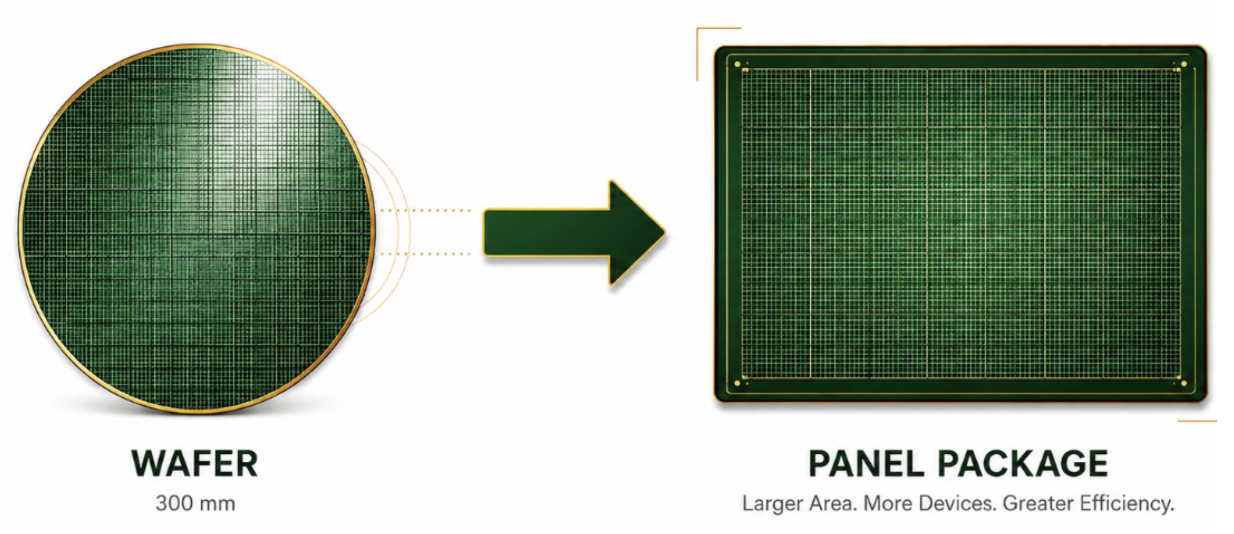
Panel-Level Packaging: The Future of Advanced Semiconductor Packaging?

The Beauty of Quantum Computing
A Brief History of Quantum Computing
While the debate between quantum and classical physics became widely publicized at the 1927 Solvay Conference — where Einstein, Bohr, and their contemporaries famously exchanged passionate arguments over the meaning of the new theory — it would not be until 1981 that the “Quantum 2.0” era truly began, when Richard Feynman championed the idea of using quantum mechanics itself to simulate nature. Shor’s algorithm then rose to fame in 1994, demonstrating that a quantum computer could factor large numbers efficiently and, in doing so, unsettling the foundations of modern cryptography and drawing the field into the mainstream imagination.
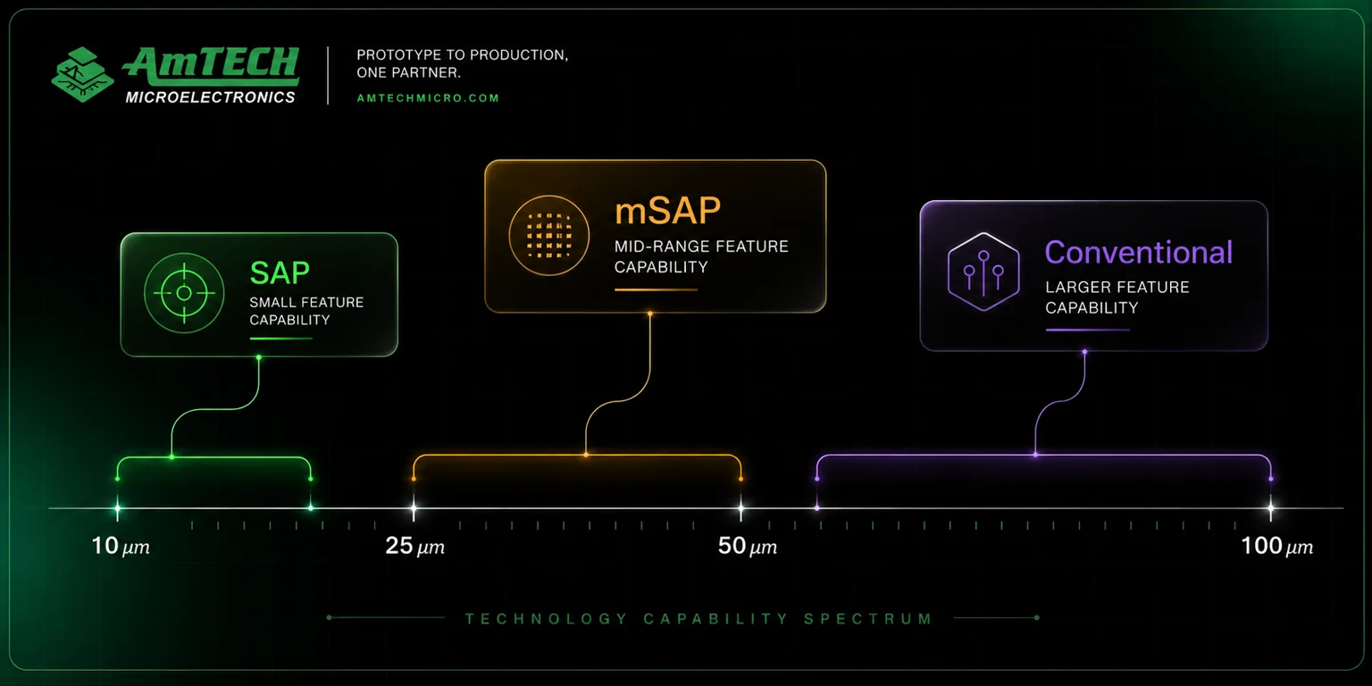
mSAP vs. Conventional PCB Fabrication
What Is mSAP?
Modified Semi-Additive Processing (mSAP) is a fabrication approach designed to overcome the limitations of traditional etching in Printed Circuit Board (PCB) industry.
Rather than beginning with a thick copper layer and removing most of it, mSAP starts with a thin copper seed layer. Copper is then selectively plated only where circuitry is required. The result is dramatically improved line definition, finer trace geometries, and higher routing density compared with conventional subtractive methods.

Crossing the Valley of Death in Semiconductor Packaging
AmTECH bridges R&D innovation with scalable, sub-micron packaging for photonics, medical, neuromorphic, quantum and DoD applications.
In today’s Industry 4.0 landscape, innovation is advancing at unprecedented speed, but many promising ideas still fail to scale beyond early prototypes. This critical gap, known as the “valley of death,” occurs when startups face the dual challenge of securing funding while needing access to advanced manufacturing capabilities.